Resin-Free Quantum Dot Color Converters

Unmet Needs

MicroLED displays are positioned to enable the next generation of near to eye display based products such as Augmented Reality and Virtual Reality headsets. They boast superior energy efficiency, fast refresh, and brightness.

However many of the high resolution microdisplays are monochrome (e.g. only emits in blue). Current methods to manufacture tri-colored microLED displays have the following unmet needs.

Poor Resolution

Expensive Capital Equipment

Poor Throughput

High Cost of Manufacturing

Our Solution

NanoPattern’s patented ink formulations addresses ALL of the unmet needs above. The ink enables the patterning of high resolution quantum dot downconverter layers allowing for low cost manufacturing of next generation displays at a fraction of the cost.

With our patented direct nanoparticle lithography process (see technology section) a display maker is able to take our ink, coat, expose with a mask and a UV light, and develop a pattern. This process is fully compatible with conventional photolithography and is a parallel patterning process.

HIGH RESOLUTION

PLUG AND PLAY

NanoPattern has demonstrated 10 by 10 micron resolution required to enable manufacturing of <800ppi direct view displays. The approach uses conventional 365 nm photolithography.

bird.png

MULTIPATTERN

To convert a blue only microLED display into a tri-colored display, there is a need to pattern both red and green quantum dots without compromising the underlayer. NanoPattern can go even further and pattern blue, green, and red without hurting the integrity of the underlayers.

HIGH EFFICIENCY

Figure - emission spectra of the patterned quantum dot film compared to the source quantum dot in solution.

Unlike other approaches, Nanopattern ink is able to preserve high conversion efficiencies at the film level even at very high packing densities that usually result in conversion loss.

Technology

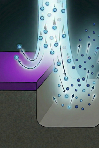
Conventionally, ligands coordinate to the surface of nanoparticles enabling them to be dispersed into varying solvents. Here at NanoPattern, we have introduced additional functionalities to this ligand. Upon irradiation with UV light (i g h line compatible) or heating, the ligand decomposes or chemically changes altering the solubility. This feature enables NanoPattern's technology to transform any nanoparticle into a photopatternable ink without the need for additional resin or photoacid generators. The key fundamental advantage of this approach is density. Compared to other approaches of photopatterning nanoparticles by suspending them in a photoresist resin or ink jet printing, NanoPattern's approach uses only the nanoparticle - by result reaching much higher packing densities. High packing density in a patterned film has many uses in the electronics industry and fully realizes the potential of nanomaterials for the next generation of electronics.

Direct nanoparticle photolithography

Image - concept drawing showing how upon irradiation by light or heat, the ligand attached to the nanocrystal decomposes or alters in chemistry allowing for a contrast in solubility.

Advantage = Density

Image - concept drawing showing the key difference in the NanoPattern approach compared to ink jet and photoresist where the functional nanocrystal is only a small fraction of the total volume.

Higher density = thinner films and higher resolution

So why does density matter? With higher density, NanoPattern’s films are able to reach an optical density of 2 desired by the display industry at less than half the thickness of what is possible today. This thickness is important because of aspect ratio. As shown in example (c) below, if 30 micron thick films are needed to reach and optical density of 2 for a 5 micron lateral resolution, this would cause resist collapse. Due to the high density, NanoPattern’s downconverter films are able to achieve a more realistic aspect ratio, allowing for sub 10 micron resolutions to be reached without resist collapse.


interested in working with us?

Contact Us